| CONTACT DATA | |
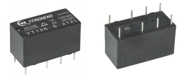
| Model | YT106 |
| Contact Arrangement | 2C |
| Contact Resistance | 100mΩ Max. |
| Contact Material | Silver Alloy |
| Contact Rating ( Res.Load ) | 1A 125VAC;2A 30VDC |
| Max. Switching Current | 2A |
| Max. Switching Voltage | 125VAC/30VDC |
| Max. Switching Power | 125VA/60W |
| Mechanical endurance | 1x10⁷ 次 OPS |
| Electrical endurance | 1x10⁵ 次 OPS |
| CHARACTERISTICS | |
| Operate Time ( at nomi.volt. ) | 6ms Max. |
| Release Time ( without diode ) | 4ms Max. |
| Insulation Resistance | 100MΩ Min.( 500VDC ) |
| Dielectric Strength | Between Open Contacts : 750VAC, 50/60Hz 1 min. |
| Between Coil & Contacts: 1,000VAC, 50/60Hz 1 min | |
| Vibration resistance | Functional: 10~55Hz 双振幅 1.5mm ( DA ) |
| Destructive: 10~55Hz 双振幅 1.5mm ( DA ) | |
| Shock resistance | Functional: 10G Min. |
| Destructive: 50G Min. | |
| Ambient Temperature | -40℃~+85℃ ( No condensation) |
| Unit Weight | Approx. 5.0g |
| COIL DATA (at 23℃) | ||||||
| Rated voltage (VDC) |
Rated current ±10%(mA) |
Coil resistance ±10%(Ω ) |
Max allowable voltage VDC (Max.) |
Operate voltage VDC (Max.) |
Release voltage VDC (Min.) |
Rated coil power (W) |
| 3 | 50.0 | 60 | 7.0 | of rated voltage75 % |
of rated voltage5 % |
approx.0.15 |
| 5 | 30.0 | 167 | 11.5 | |||
| 6 | 25.0 | 240 | 13.8 | |||
| 9 | 16.7 | 540 | 20.8 | |||
| 12 | 12.5 | 960 | 27.7 | |||
| 24 | 6.3 | 3,840 | 55.2 | |||
| 3 | 66.7 | 45 | 6.0 | of rated voltage75 % |
of rated voltage5 % |
approx.0.20 |
| 5 | 40.0 | 125 | 10.0 | |||
| 6 | 33.3 | 180 | 12.0 | |||
| 9 | 22.2 | 405 | 18.0 | |||
| 12 | 16.7 | 720 | 24.0 | |||
| 24 | 8.3 | 2,880 | 48.0 | |||
| 3 | 120.0 | 60 | 4.5 | of rated voltage75 % |
of rated voltage5 % |
approx.0.36 |
| 5 | 72.0 | 167 | 8.0 | |||
| 6 | 60.0 | 240 | 10.0 | |||
| 9 | 40.0 | 540 | 14.5 | |||
| 12 | 30.0 | 960 | 18.5 | |||
| 24 | 15.0 | 3,840 | 35.5 |
| ORDERING INFORMATION | |
| Type designation : | YT106 |
| Protective construction : | S-Flux proofed |
| Number of poles : | 2-2 Group |
| Coil voltage : | 03,05,06,09,12,24 (VDC) |
| Coil power: | D-0.36 W,L-0.2W
(0.15W optional) |
| Contact form : | Nil-Form C |
| Outline Dimensions | PCB Layout (Bottom View) | Wiring Diagram( Bottom View) |
 |
 |
 |